Chapter 2.8 — Foundry & Fabrication
A brilliant design is not a product until a foundry can manufacture it at acceptable yield, cost, and volume. That conversion—not the process-node label alone—is what customers pay for. The foundry advantage compounds through customer learning, while its economics still turn on utilization, yield, and the price paid for geographic resilience.
A foundry manufactures chips designed by companies such as Nvidia, AMD, Apple, and the hyperscalers. A leading-edge fab costs more than $20B and may take years to reach acceptable yield, the fraction of working chips on a wafer. It uses the extreme-ultraviolet lithography described in Chapter 2.9 to print features only a few nanometers wide. Progress is organized by process nodes such as 3nm and 2nm. Each new node now costs more while delivering smaller economic gains, increasing the importance of the memory and packaging discussed in Chapter 2.7.
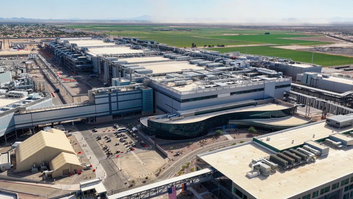
Yield is the bridge between technology and economics. Suppose a wafer contains one hundred potential dies. If only fifty are usable, every good die must absorb the cost of the entire wafer and the fifty failures. If ninety are usable, the same manufacturing input produces almost twice as many saleable chips. A small improvement in yield can therefore change customer cost and foundry margin dramatically, especially when each die is large and the wafer is processed through hundreds of expensive steps.
Yield also develops over time. Early production reveals defects, equipment interactions, and design rules that were not visible in the laboratory. Engineers adjust the process, customers alter layouts, and the share of working dies rises. A foundry serving many demanding customers receives more learning cycles and can spread development cost over more volume. That creates a feedback loop: better yield attracts customers; more customers generate learning and cash; learning and cash fund the next process.
For the customer, the product is not “2 nanometers.” It is a known number of good dies, delivered on schedule, at a cost and power level the final system can support. Process labels are useful shorthand, but they do not make different foundries economically equivalent. This chapter therefore follows the conversion from design tape-out to repeatable volume rather than treating a node announcement as the finish line.
Why a strong design can still fail to become a saleable product
A design becomes a saleable product only when a fab can print it repeatedly at acceptable yield. At the leading edge, almost every major designer depends on the same manufacturing system, so that execution risk is also a concentration risk.

TSMC generated about $40.2B in revenue in the second quarter of 2026, its 2nm node entered volume production and is sold out through the year, and it plans a roughly 70% compound growth in advanced-node capacity through 2028. Its share of the pure-play foundry market dwarfs everyone else's.12

Only three foundries are in the 2 nm-class race
Only a handful of companies can make a modern chip at all, and only three are in the 2nm-class race.
| Foundry | Ticker | Leading node | Status |
|---|---|---|---|
| TSMC | TSM | N2 (2nm) → A16 | ~90% of leading-edge; sold out |
| Samsung Foundry | 005930.KS | SF2 (2nm) | credible #2; Tesla AI6 win |
| Intel Foundry | INTC | 18A → 14A | tech leads (PowerVia, High-NA); few external customers |
| SMIC | 688981.SH / 0981.HK | 7nm (via DUV) | China champion; ~20–30% yield |
| GlobalFoundries | GFS | mature nodes | US-based, not leading-edge |
| UMC | UMC | mature nodes | trailing-edge specialist |
The table contains two different markets. TSMC, Samsung, and Intel are attempting the most advanced logic, where process-development cost, yield, and anchor customers determine success. GlobalFoundries and UMC focus on mature processes used in communications, automotive, industrial, and many supporting chips. Mature nodes can be attractive businesses, but they do not substitute for the leading-edge capacity needed by frontier accelerators.
SMIC occupies a third position. It is strategically essential to China and can manufacture advanced-enough domestic products using older tools and more process steps. That can satisfy a national availability objective while producing a higher cost per good die. A policy-backed foundry should therefore be judged both as an industrial capability and as a security: national importance can sustain investment even when conventional returns are weak, but it does not erase yield and depreciation.
The 2 nm race is ultimately an economics race
The leading edge is a three-way contest with diverging strategies. TSMC's N2 node entered volume production in late 2025 and ramps through 2026, its first gate-all-around transistor, with backside power delivery arriving in the A16 node in the second half of 2026; TSMC is deliberately deferring the ultra-expensive High-NA lithography tool, betting that mature machines keep its cost per transistor lower for longer. Intel took the opposite bet: its 18A node reached volume in mid-2025 with backside power (PowerVia), beating TSMC to it, and Intel was the first to put a production High-NA machine to work, genuine technology leads. But Intel Foundry still lacks a TSMC-scale roster of external customers, which is the one thing that would make its comeback real, and its 14A node will be more expensive precisely because of High-NA. Samsung's SF2 process reached above 60% yield and landed a $16.5B Tesla contract as validation, though the AI6 chip reportedly slipped as 2nm production lagged.
The timing of High-NA lithography will shape leading-edge economics for years. Intel is adopting it early in an attempt to gain process advantage, TSMC is deferring it to control cost, and ASML (Chapter 2.9) supplies either strategy. As node shrinks deliver smaller gains at higher cost, a larger share of system performance depends on the packaging and memory discussed in Chapter 2.7.
Overseas fabs reduce risk without recreating Taiwan's ecosystem
The United States leads chip design but does not yet host volume leading-edge manufacturing; that capacity remains concentrated in Taiwan. TSMC is diversifying through an Arizona program of around $265B, including planned 2nm fabs, plus sites in Japan and Germany. The shift is slow: Arizona remains behind Taiwan's initial ramp, while much advanced packaging and research and development stay in Taiwan. A disruption in the Taiwan Strait would therefore interrupt the AI supply chain, and current overseas construction does not remove that exposure before roughly 2030.
China sits on the other side of the same wall. Its national foundry, SMIC, produces 7nm-class chips using older deep-ultraviolet tools and multi-patterning, the workaround for being denied EUV, but at yields estimated in the 20–30% range that make the economics dependent on state support. SMIC is the manufacturing ceiling on China's entire AI-chip ambition: the Ascend and Cambricon accelerators of Chapter 2.5 can only ship in the volumes SMIC can yield, and pushing below 7nm on purely domestic equipment is judged unlikely before the end of the decade, though a SiCarrier-affiliated domestic immersion tool is in testing at SMIC toward a 28nm domestic flow in 2027. Fabrication and high-bandwidth memory are the two hard limits on Chinese AI, and this is one of them.
Geographic diversification should be understood as insurance with a cost. A new overseas fab requires duplicate infrastructure, a trained workforce, local suppliers, and time to reach the efficiency of the original site. Subsidies can move equipment and some production, but they cannot instantly move decades of tacit process knowledge or the surrounding packaging and materials ecosystem. The result can be greater resilience alongside a higher cost per wafer and lower early utilization.
That trade-off is rational for governments and customers that value continuity, but it changes the foundry’s return calculation. The investor needs to know who pays the resilience premium: the customer through higher wafer prices, the government through subsidies, or the foundry through weaker margins. “More capacity outside Taiwan” is not enough to answer that question.
TSMC's advantage is a learning loop of yield, customers, and cash
A foundry's moat is expressed through economics as much as transistor density. New fabs absorb capital years before they generate revenue; low initial yields consume wafers without producing saleable dies; and fixed depreciation makes utilization a powerful driver of margins. A node can be technically competitive yet economically weak if it lacks enough anchor customers to fill the fab and spread process-development cost. Conversely, a dense portfolio of customers supplies learning cycles, purchasing scale and cash to finance the next node.
That feedback loop explains the difference between process announcements and a durable foundry franchise. For TSMC, the key questions are pricing, leading-edge utilization, customer concentration and returns on overseas capacity. For Intel and Samsung, the decisive evidence is not a demonstration wafer but repeat external volume from customers that are not affiliated with the foundry owner. Capacity announcements should therefore be read with a lagged-normalization risk: synchronized subsidies can create excess capacity in mature nodes even while the leading edge remains scarce.
External customers turn process claims into evidence
ASML's High-NA orders show which manufacturers are committing to early adoption. TSMC's 2nm and A16 yields and Arizona schedule indicate whether its lead is narrowing. An external leading-edge customer for Intel Foundry would establish commercial competition; Samsung must demonstrate stable yields and retention of its Tesla program; SMIC's yields determine how quickly China can scale domestic AI chips. Across all four, smaller gains from node shrinks increase the importance of packaging and memory.
One wafer can support very different economics
Two foundries can process the same number of wafers and produce very different economics. A plant with high yield, several external customers, and reliable delivery creates more saleable output and higher-quality revenue than one with lower yield, an affiliated anchor customer, and continuing subsidies. Nominal capacity alone does not measure either competitive position or return on capital.
Yield affects more than unit cost. A large accelerator die occupies substantial wafer area, so a defect can destroy an expensive unit and reduce the number of good dies from the whole wafer. Lower yield also consumes packaging and test resources on parts that may never become revenue. As engineers identify defect sources, adjust process recipes, and feed the result back into production, yield improves. A foundry serving many demanding customers can run this learning loop more often and spread the cost across more volume.
This is why an external-customer win carries information beyond the announced order. The customer has trusted the process design kit, committed engineering resources to the node, and accepted the foundry’s manufacturing roadmap. Repeat volume then shows that the economics survived qualification. By contrast, a chip produced for the foundry owner’s internal product proves technical capability but provides less evidence about price, service quality, or the willingness of independent designers to accept lock-in.
For an investor, the accounting sequence is long. Capital spending and equipment installation come first. Qualification wafers and early production may follow without attractive utilization. Customer revenue appears when volume ramps, while depreciation from the new fab can pressure margin before the line fills. A government subsidy may lower the capital burden but cannot create customers or good dies. The cleanest foundry thesis therefore connects node demand, external designs, yield, utilization, pricing, depreciation, and packaging capacity rather than stopping at the node label.
Strategic necessity still faces a purchase price
TSMC (TSM) is presently difficult to substitute at the leading edge and sits upstream of Nvidia, Apple, AMD, and Broadcom. That strategic position supports pricing power, but security attractiveness still depends on valuation and the uncompensated Taiwan tail risk. Intel (INTC) is a high-variance US alternative, with genuine process capability and a government backstop but unproven external foundry demand; Samsung (005930.KS) is the credible second source; GlobalFoundries (GFS) is a US-based mature-node exposure. The equipment makers in Chapter 2.9 diversify foundry-customer risk but remain cyclical. On the Chinese side, SMIC (688981.SH, 0981.HK) is the mandated national champion, while low leading-edge yield makes it primarily a policy and localization thesis rather than a conventional margin thesis.
The event no portfolio can fully diversify
The dominant risk here is not competitive but geopolitical: a Taiwan Strait crisis is the single event that would invalidate the entire AI capex thesis in this atlas at once, and it can be sized but not hedged away. Short of that, the TSMC thesis would weaken if Intel Foundry genuinely won external leading-edge customers at scale, introducing real competition for the first time in years, or if Arizona and the other overseas fabs de-risked Taiwan faster than expected. The China thesis changes if SMIC breaks its yield ceiling or acquires a domestic path below 7nm, which would loosen the manufacturing limit on Chinese AI chips and pressure the allied advantage that this layer, like memory, currently represents.
For the platform-level distinction between confirmed fabrication, reported relationships and undisclosed next-generation allocation, see §2.13.
The ordinary monitoring case is less dramatic than the tail risk. For TSMC, watch leading-edge utilization, pricing, yield progression, advanced-packaging coordination, and the margin cost of overseas production. For Intel and Samsung, watch repeat external customers rather than internal products or technology demonstrations. For SMIC, watch good-die output and sustainable volume, not only process claims.
Across all four, compare the same boundary: good external volume produced at an economic yield. That common measure avoids mistaking a technology demonstration, installed clean-room capacity, or subsidized strategic output for an equally mature commercial foundry business.
The investment conclusion is that foundry power comes from repeatable conversion. A designer can change a block of code in weeks; moving a leading product to another manufacturing process can require years of redesign, qualification, and yield learning. That switching friction gives the incumbent extraordinary delivery power. But a capital-intensive moat still has a price: underutilized fabs, subsidized duplication, customer concentration, or geopolitical disruption can overwhelm the strategic value. The winning process is the one that produces enough good chips for customers and enough return on capital for shareholders.
Sources
Linked evidence for this chapter's figures and load-bearing claims: 1 2