Chapter 2.9 — Equipment & EDA
Chipmakers do not buy tools merely to own machines; they buy repeatable yield. Equipment and design software earn their moat through years of process integration, installed-base service, and qualification. That makes this layer unusually durable—but also cyclical, politically exposed, and vulnerable when customers pull orders forward.
Chip production depends on physical systems that deposit, etch, coat, and inspect silicon—collectively wafer-fab equipment (WFE)—and on electronic design automation (EDA) software. The WFE market is about $116B a year and is growing with AI-related memory and logic demand. A small number of suppliers control critical process steps, creating high margins, customer dependence, and a powerful channel for export controls.
A finished chip is created by repeating a cycle on a silicon wafer. Material is deposited, coated with a light-sensitive chemical, patterned by lithography, etched away, cleaned, measured, and then layered again. The cycle may occur hundreds of times. A defect introduced early can make a later step useless; a small change in one machine can alter the recipe required by several others. The equipment is therefore part of a production system, not a collection of independent tools.
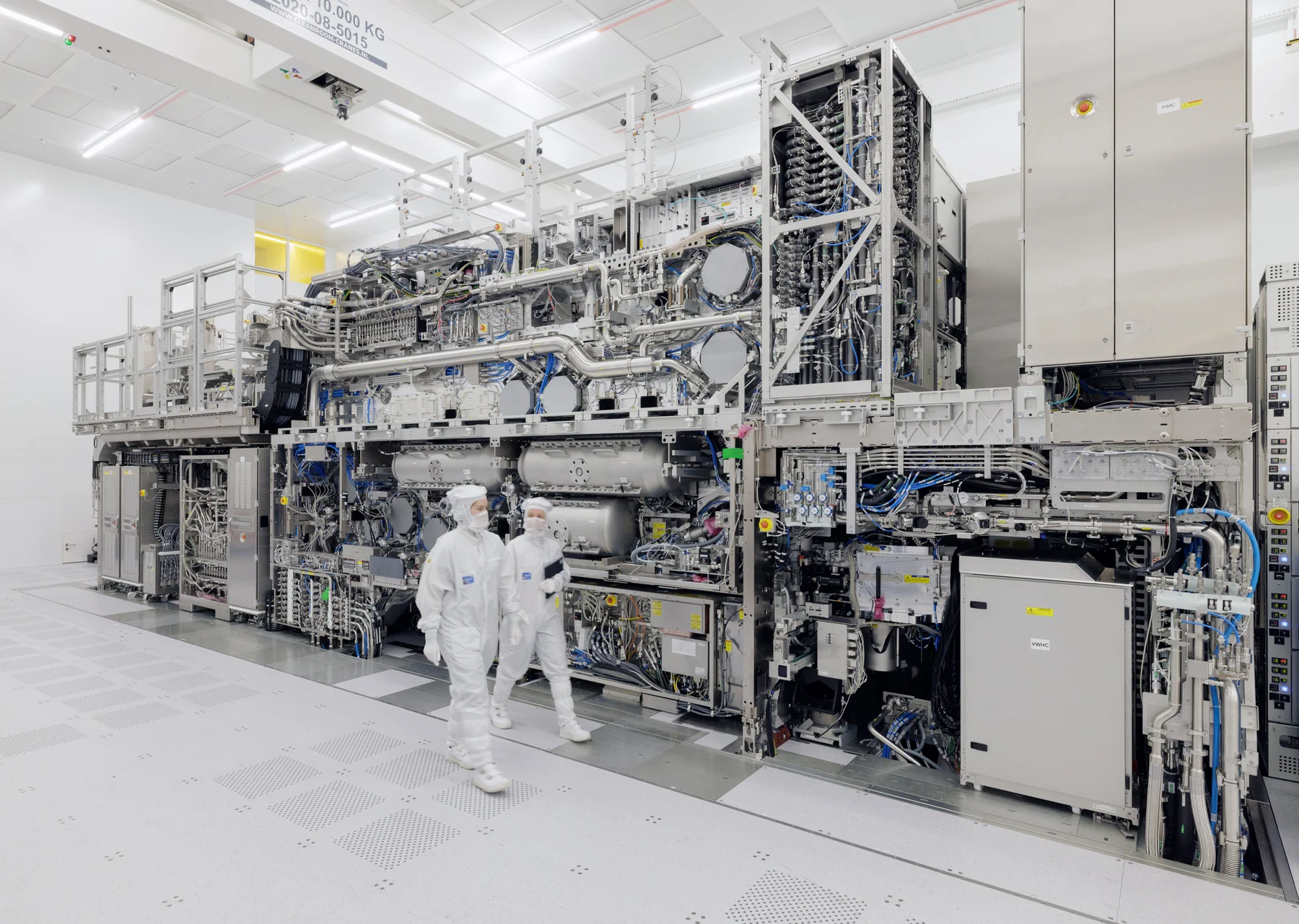
The customer is paying for process certainty. A fab wants the machine to reproduce the same result across wafers, shifts, and years, and it wants the vendor to diagnose deviations before yield collapses. That demand explains why service engineers, process data, spare parts, and software matter almost as much as the original tool. A technically plausible substitute is not commercially equivalent until it has survived qualification inside the customer’s production flow.
EDA sits at the beginning of the same chain. Engineers use design software to describe the chip, place billions of transistors, verify timing and power, test whether the design can be manufactured, and prepare the final files sent to the foundry. An error discovered before fabrication can be corrected in software. An error discovered after tape-out can waste months and an expensive production run. EDA earns its value by preventing that outcome and by translating a design into the rules of a specific manufacturing process.
The factory depends on five process leaders and one monopoly
The equipment market divides cleanly, with each of the five giants owning a step of the process.

The most important of them is ASML. It is the sole maker of extreme-ultraviolet (EUV) lithography machines, the systems that print the finest features on a leading-edge chip, and its monopoly is total: no EUV, no advanced logic or memory. Its next-generation High-NA machine costs roughly $350–400M each, and the first units have gone to Intel, SK Hynix, and Samsung. Applied Materials and Lam Research dominate the deposition and etch steps, Tokyo Electron holds about 91% of the coater-developer niche, and KLA controls process-control and inspection with more than 85% of the optical-inspection market. Because each owns its step, they do not so much compete with one another as ride the same wave of fab construction together.
The value chain sells process certainty
The roster spans lithography, the process-step leaders, the design-software duopoly, the advanced-packaging machine makers, and the Chinese localization champions.
| Player | Ticker | Role |
|---|---|---|
| ASML | ASML | lithography — 100% of EUV |
| Applied Materials | AMAT | deposition, ion implant, CMP |
| Lam Research | LRCX | etch + memory deposition |
| Tokyo Electron | 8035.T | coater/developer, etch, clean |
| KLA | KLAC | metrology & inspection |
| Synopsys, Cadence | SNPS, CDNS | EDA design software (the duopoly) |
| Besi, ASMPT, Kulicke & Soffa | BESI, 0522.HK, KLIC | advanced-packaging / bonding equipment |
| Naura, AMEC, Hwatsing | 002371.SZ, 688012.SH, 688120.SH | China WFE (etch, deposition, CMP) |
| SMEE, SiCarrier | (China, private/listed) | China lithography (DUV; the gap) |
| Empyrean, Primarius | 301269.SZ, 688206.SH | China EDA |
The companies are not interchangeable exposures to one equipment cycle. ASML owns a unique lithography monopoly. Applied Materials and Lam participate across many process steps and customer types. KLA sells the measurement and inspection needed to find defects as structures become harder to see. Tokyo Electron combines several process positions. EDA vendors sell recurring software and intellectual property rather than factory machines. Packaging-equipment makers depend on a later stage of the value chain.
Their revenue also arrives differently. A new tool may be ordered when a fab is planned, shipped when the building is ready, accepted only after installation and testing, and followed by years of service. EDA contracts renew while engineers continue to design. A headline increase in fab investment can therefore affect backlog, revenue, and cash at different times across the group. Comparing the companies requires matching the order stage to the accounting line.
EDA becomes more valuable as design complexity rises
The design-software layer is a story of concentration as extreme as the equipment.

Synopsys and Cadence, the two American EDA leaders, together hold well over half the market, with Siemens EDA a distant third, and their software is so embedded in how chips are designed that switching is nearly unthinkable; both are increasingly weaving AI into the design process itself, with tools like Synopsys's DSO.ai and Cadence's Cerebrus. It is a duopoly with the pricing power that implies, and, like the lithography layer, a weapon: when the US briefly required export licenses for chip-design software to China in 2025, Synopsys suspended its guidance and halted China sales overnight, before the rule was rescinded weeks later in a trade truce. China's own EDA champions, Empyrean and Primarius, hold only about a tenth of their home market and lack a full-flow tool suite for the most advanced nodes.
AI can improve this software without automatically destroying the moat. It can search a larger design space, suggest placement, and reduce the time engineers spend on repetitive optimization. But the result still has to satisfy physical rules, integrate with foundry process files, and pass verification. A new AI-native interface is not a substitute for the accumulated models, customer trust, and manufacturing integration inside the established flow.
The investment risk is subtler. If AI makes engineers more productive, customers can design more chips and purchase higher-value tools. If it eventually makes parts of the flow interchangeable, it can reduce switching friction. The evidence to watch is not the number of AI features launched. It is whether customers expand spending, tape out designs faster, and continue to standardize on the same full-flow platform.
Equipment is the most precise technology-policy lever
This layer is where the US and its allies hold their most decisive leverage over China, and where they have used it. China has pushed its equipment self-sufficiency to roughly 35%, and its national champions have grown fast: Naura has climbed to about the fifth-largest equipment maker in the world, its revenue heading toward $7B, and AMEC's etch tools approach the cutting edge. But the gap that matters is lithography. China has no domestic EUV; its most advanced homegrown machine, from SMEE, does older deep-ultraviolet work, and while a SiCarrier-affiliated immersion-DUV tool is being tested at SMIC toward a 28nm domestic flow in 2027, integration into a production line at scale is years out. Denying China EUV is what caps SMIC's fabrication ceiling in Chapter 2.8, and denying it the servicing and spares for the tools it already owns is a newer, quieter escalation that the US has pressed the Netherlands and Japan to join. The exposure runs both ways, though: China is a large customer, historically around a fifth of Cadence's revenue and a meaningful slice of ASML's (guided down toward 20% for 2026), so the same controls that constrain China also cost the toolmakers.
Advanced packaging creates a second equipment cycle
A newer growth vector inside this layer is the equipment for advanced packaging, driven by the CoWoS bottleneck of Chapter 2.7. As TSMC quadruples its packaging capacity, demand flows to the makers of the bonding and assembly machines: Besi, whose hybrid-bonding tools are central to the next generation and which runs a joint venture with Applied Materials; ASMPT and Kulicke & Soffa; and Applied Materials itself. High-bandwidth memory intensifies this, because a bit of HBM consumes roughly three times the wafer-fab capacity of a bit of ordinary memory, so the AI build drives disproportionate equipment demand at exactly the packaging and memory steps where value is concentrating.
Installed base and qualification turn sales into recurring economics
Equipment economics extend beyond the initial tool sale. A qualified process tool generates spare-parts, service, software and upgrade demand over a long installed life, making the installed base a stabilizer when new-fab spending slows. Process control and lithography can be especially sticky because changing a tool alters the process recipe and may force costly requalification. Technical service intensity, installed-base growth and recurring revenue therefore deserve separate attention from annual wafer-fab-equipment shipments.
The same stickiness does not remove cyclicality. Customers can pull equipment forward ahead of an export-control deadline, double-order during a shortage or pause once a fab shell has been equipped. A strong shipment quarter can therefore borrow from the future. The underwriting sequence should be: end-market wafer demand, customer utilization, fab construction, tool orders, revenue recognition and finally service attachment. SEMI's equipment forecast is an industry spending measure, not a promise of identical growth or margins for every vendor.1
Customer concentration and geographic mix are equally important. China restrictions can remove addressable products while localization spending temporarily raises demand for permitted tools. Memory suppliers' synchronized expansions can create a sharp up-cycle followed by digestion. The most defensible suppliers are those whose process step becomes more intensive at each node, whose installed bases compound, and whose tools remain difficult to replace without yield loss.
Orders must distinguish real expansion from pull-forward
The defining technical question is the timing of High-NA lithography, the same debate as in Chapter 2.8, and ASML's order flow is a clean read on who is betting what. Watch China's self-sufficiency percentage and whether it can finally close the lithography gap; watch the export-control and servicing rules for further escalation or relaxation; watch the packaging-equipment makers as CoWoS capacity keeps expanding; and watch the WFE cycle itself, because this layer is cyclical and a downturn would hit all five giants together regardless of the AI narrative.
The sequence matters. Foundry utilization and end demand justify a capacity plan. The customer then secures a fab shell, utilities, and tools. Orders become backlog before shipments; shipments may precede customer acceptance; service revenue follows the installed base. Export deadlines can pull several stages forward without changing long-run wafer demand. A quarter of exceptional orders can therefore be a sign of confidence, defensive stockpiling, or demand borrowed from the next year.
To distinguish them, compare orders with customer capital budgets, fab construction progress, tool lead times, cancellation terms, and subsequent utilization. Healthy expansion produces working capacity that remains full. Pull-forward produces an air pocket after customers finish equipping or discover that end demand cannot absorb the output.
Which companies retain the economics
ASML (ASML) is the supply chain's most concentrated lithography chokepoint, with China exposure and the timing of leading-edge capacity as major swing factors. Applied Materials (AMAT), Lam Research (LRCX), KLA (KLAC), and Tokyo Electron (8035.T) diversify across process steps and customers, but remain exposed to wafer-fab-equipment normalization. Synopsys (SNPS) and Cadence (CDNS) form the EDA duopoly and carry software-like recurrence alongside semiconductor-cycle exposure. Besi (BESI) is a more concentrated packaging-equipment expression. Naura (002371.SZ) and AMEC (688012.SH) are Chinese localization beneficiaries, with Entity List exposure and a persistent domestic-lithography ceiling. None of these strategic positions eliminates entry-valuation risk.
The timing of these exposures is different enough to matter. EDA revenue begins while a chip is still being designed and can recur through multiyear licenses. Equipment orders arrive when the fab commits to capacity, but shipment, installation, customer acceptance, and revenue recognition can span several reporting periods. Service grows after the installed base begins production. A single AI-platform launch can therefore reach software, tool, and service suppliers in different quarters even when all ultimately support the same chip.
That sequence helps interpret a slowdown. Falling new-tool orders can coexist with healthy service revenue because existing fabs still need maintenance, parts, process tuning, and upgrades. EDA can remain resilient while customers reduce tape-outs at the margin because switching the core design environment would be disruptive. Conversely, a surge in construction announcements may not support near-term revenue if permits, utilities, export licenses, or customer acceptance delay the physical tools. Investors should match each company to the stage where it gets paid rather than using one industry capex headline for the entire layer.
China exposure can amplify both the boom and the reversal
The equipment thesis is cyclical at its core, so the main risk is a WFE downturn, which would affect all five giants despite the AI narrative. ASML's specific exposure is China: tighter export controls could remove addressable revenue, while relaxation would add to it. A credible Chinese breakthrough in domestic lithography would gradually weaken a central allied point of leverage over advanced Chinese chipmaking. The EDA duopoly would also face a new question if AI-driven design tools lowered the barrier to a credible competitor, although current evidence does not establish such a challenger.
For how these upstream production constraints surface in the four anchor accelerator and AI-factory systems, see §2.13.
The chapter’s conclusion is to separate structural moat from cyclical timing. Qualification, process data, installed service, and EDA integration can make a supplier extremely difficult to replace. Those advantages do not prevent customers from pausing orders after a spending surge. The best company in the layer can still produce a poor return if the investor buys at peak backlog and peak valuation just before utilization falls.
A disciplined review starts with wafer demand and customer utilization, moves to announced capacity and construction, then to orders, shipments, acceptance, and service. It separately tracks export rules and domestic substitution, because policy can redirect the same order book before industry demand changes. The company earns its moat by making yield repeatable. The investor earns a return only if that moat is purchased at a point in the equipment cycle when future orders have not already been fully anticipated.
Sources
Linked evidence for this chapter's figures and load-bearing claims: 2 1 3 4 5 6 7
Footnotes
-
SEMI Reports Global Total Semiconductor Equipment Sales Forecast to Reach $125.5 Billion in 2025. SEMI, 2025-07-22; accessed 2026-07-25. ↩ ↩2
-
Applied Materials Announces Second Quarter 2026 Results. Applied Materials, 2026-05-14; accessed 2026-07-25. ↩
-
Financial results. ASML, 2026-01-28; accessed 2026-07-25. ↩
-
Quarterly Reports: quarter ended March 31, 2026. KLA, 2026-04-30; accessed 2026-07-25. ↩
-
Lam Research Reports Financial Results for the Quarter Ended March 29, 2026. Lam Research, 2026-04-22; accessed 2026-07-25. ↩
-
FY2026 Annual Results. Tokyo Electron, 2026-04-30; accessed 2026-07-25. ↩